
Microscale
SN74LS73N IC
SN74LS73N IC
Couldn't load pickup availability
What it is
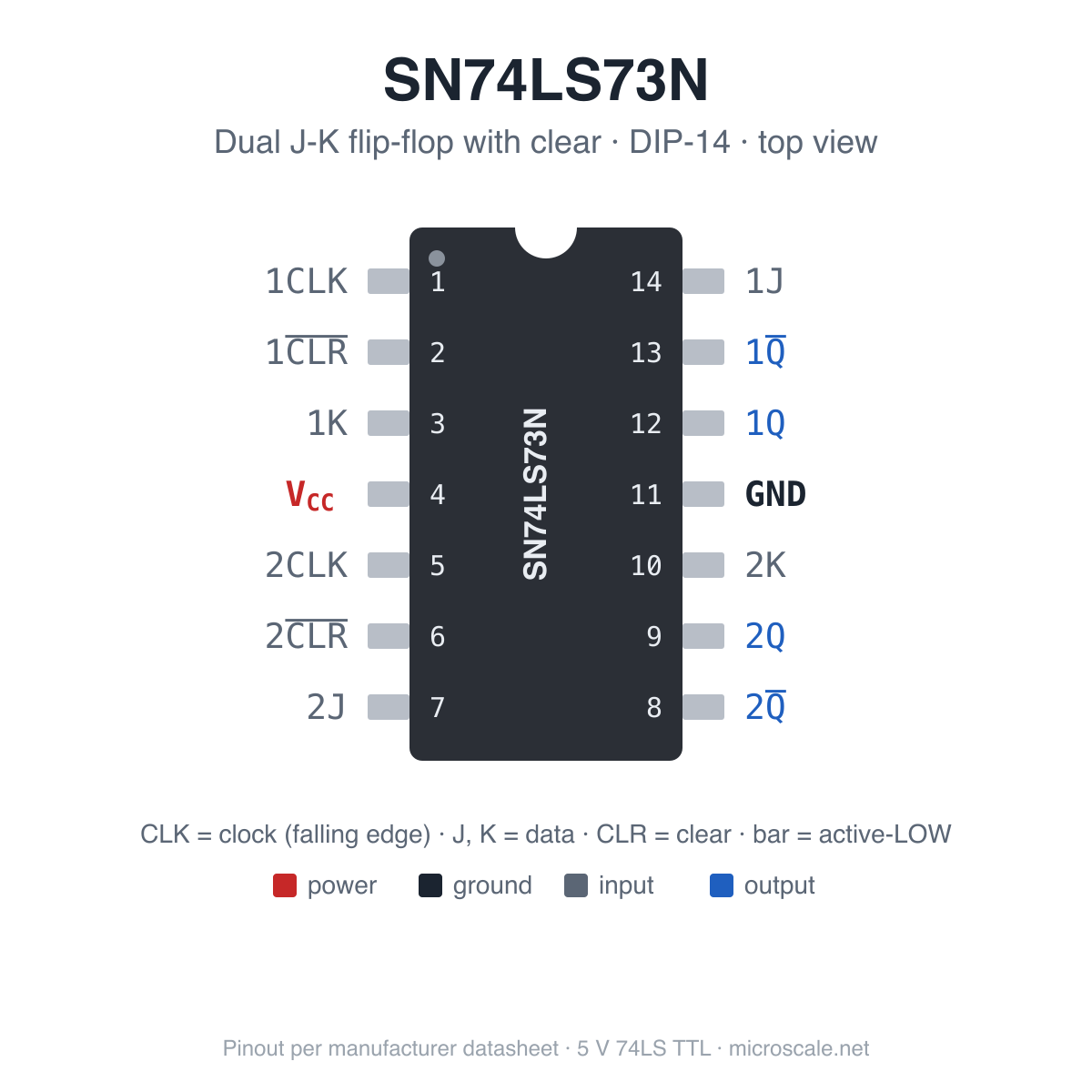
The SN74LS73N has two independent J-K flip-flops in a 14-pin DIP. Each has its own clock, J and K inputs, Q and Q outputs, and an active-LOW clear input. Outputs change on the falling edge of the clock. It is a 1-bit memory cell and the basic part for counters, frequency dividers and simple state machines.
⚠ Power pins are not in the corners. On this chip VCC is pin 4 and GND is pin 11. If you wire it like a 74LS00 (GND 7, VCC 14), power goes to an output and an input. Check twice before switching on.
Function table (each flip-flop)
| CLR | CLK | J | K | Q | Q | Mode |
|---|---|---|---|---|---|---|
| L | X | X | X | L | H | Clear (async reset) |
| H | ↓ | L | L | Q0 | Q0 | Hold |
| H | ↓ | H | L | H | L | Set |
| H | ↓ | L | H | L | H | Reset |
| H | ↓ | H | H | Q0 | Q0 | Toggle |
| H | H | X | X | Q0 | Q0 | No change |
↓ = falling (HIGH-to-LOW) clock edge. X = don't care. Q0 = previous state.
Pinout (DIP-14, top view, notch at the top)
| Pin | Signal | Function | Pin | Signal | Function |
|---|---|---|---|---|---|
| 1 | 1CLK | FF1 clock (falling edge) | 14 | 1J | FF1 J input |
| 2 | 1CLR | FF1 clear, active-LOW | 13 | 1Q | FF1 inverted output |
| 3 | 1K | FF1 K input | 12 | 1Q | FF1 output |
| 4 | VCC | +5 V supply | 11 | GND | Ground |
| 5 | 2CLK | FF2 clock (falling edge) | 10 | 2K | FF2 K input |
| 6 | 2CLR | FF2 clear, active-LOW | 9 | 2Q | FF2 output |
| 7 | 2J | FF2 J input | 8 | 2Q | FF2 inverted output |
Specifications
| Parameter | Value |
|---|---|
| Logic family | 74LS (low-power Schottky TTL) |
| Function | Two independent J-K flip-flops, negative-edge-triggered, with clear (no preset) |
| Package | DIP-14 (PDIP, through-hole) |
| Supply voltage (VCC) | 4.75 V min / 5 V nom / 5.25 V max |
| Absolute max supply / input voltage | 7 V |
| Input HIGH threshold (VIH) | 2.0 V min |
| Input LOW threshold (VIL) | 0.8 V max |
| Output HIGH voltage (VOH) | 2.7 V min / 3.4 V typ at −0.4 mA |
| Output LOW voltage (VOL) | 0.35 V typ / 0.5 V max at 8 mA |
| Output current | −0.4 mA source (HIGH) / 8 mA sink (LOW) |
| Clock frequency | 0–30 MHz guaranteed (fmax 30 MHz min, 45 MHz typ) |
| Propagation delay (clock / async input → Q, Q) | 15 ns typ / 20 ns max (2 kΩ, 15 pF) |
| Setup time (J, K before clock ↓) | 20 ns min |
| Hold time (after clock ↓) | 0 ns |
| Minimum pulse width | CLK HIGH 20 ns · CLR LOW 20 ns |
| Supply current (whole chip) | 4 mA typ / 6 mA max |
| Input current (LOW) | J, K: −0.4 mA max · CLR, CLK: −0.8 mA max |
| Operating temperature | 0 °C to 70 °C |
Using flip-flops
- Tie CLR HIGH for normal operation. They are active-LOW. If one floats or is pulled LOW, it overrides the clock and the flip-flop looks "stuck". This is the most common reason these chips seem dead.
- Debounce switches before they reach CLK. A mechanical push-button bounces and produces several clock edges per press, so a toggle circuit appears to skip. Use an RC filter plus a Schmitt trigger (74LS14) or an SR latch built from two 74LS00 gates.
- Divide-by-2 / toggle: tie J and K HIGH. Q flips on every falling clock edge, so Q runs at half the clock frequency.
- Ripple counter: with J = K = HIGH, feed flip-flop 1's Q into flip-flop 2's CLK to get a 2-bit binary counter (÷4). Chain more chips for more bits.
Wiring it up
- 5 V only. 74LS is TTL logic and needs 4.75–5.25 V on VCC. It will not run reliably from 3.3 V.
- Decouple it. Put a 100 nF ceramic capacitor between VCC and GND, as close to the chip as you can.
- Don't leave inputs floating. An open TTL input usually reads HIGH, but it picks up noise and gives random glitches. Tie unused inputs to VCC (directly or through 1 kΩ) or to GND.
- Arduino Uno / Nano / Mega (5 V): connect directly, no level shifting needed.
- ESP32, Raspberry Pi, STM32 and other 3.3 V boards: a 3.3 V output driving a 74LS input is fine (HIGH threshold is 2.0 V). The other direction is not: a 74LS output can sit around 3.4–3.6 V when HIGH, which is above what 3.3 V-only pins accept. Use a divider (1 kΩ in series, 2 kΩ to GND) or a level shifter, or use the 74HC/74HCT version of the chip instead.
- Driving LEDs: 74LS outputs sink current (8 mA) much better than they source it (0.4 mA). Wire the LED and a 680 Ω–1 kΩ resistor from +5 V to the output, so the LED lights when the output is LOW.
In the package
1 × SN74LS73N in a 14-pin plastic DIP (through-hole, 2.54 mm pin pitch, 7.62 mm / 0.3" row spacing). It drops straight into a breadboard across the centre channel. For soldered builds, use a DIP socket so the chip can be swapped.
The markings depend on the batch: you may get Texas Instruments (SN74LS…N), Hitachi/Renesas (HD74LS…P) or another second-source maker. They are all the same standard 74LS part: same pinout, same logic, same 5 V ratings.
Which J-K flip-flop do I need?
- SN74LS73N (this chip): clear only, 14 pins. Choose it when you only need to reset.
- SN74LS76N: adds an active-LOW preset (set), 16 pins. It also has non-corner power pins (VCC 5, GND 13).
- SN74LS112N: preset and clear, 16 pins, standard corner power (VCC 16, GND 8). This is the easiest of the three to lay out.
Datasheet