
Microscale
SN74LS76N IC
SN74LS76N IC
Couldn't load pickup availability
What it is
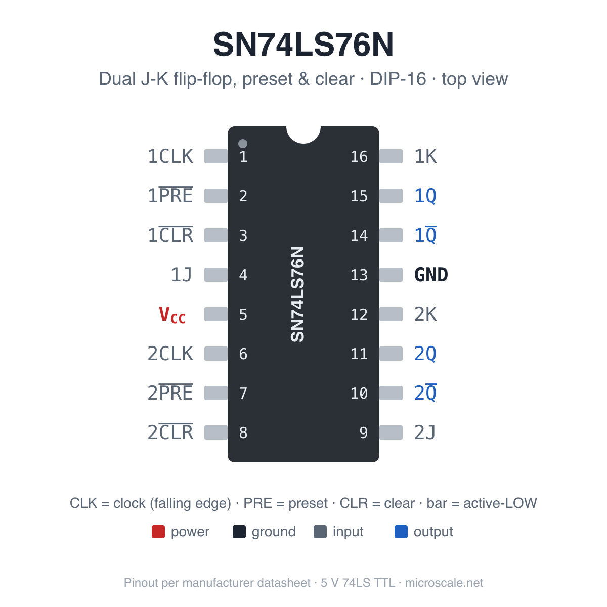
The SN74LS76N has two independent J-K flip-flops in a 16-pin DIP. Each has its own clock, J and K inputs, Q and Q outputs, and active-LOW preset and clear inputs that set or reset the output immediately, whatever the clock is doing. Outputs change on the falling edge of the clock. It is the classic textbook J-K flip-flop for counters, dividers and sequential-logic labs.
⚠ Power pins are not in the corners. On this chip VCC is pin 5 and GND is pin 13. Wiring power to pins 8 and 16, as on most 16-pin logic chips, will not work and can damage it.
Function table (each flip-flop)
| PRE | CLR | CLK | J | K | Q | Q | Mode |
|---|---|---|---|---|---|---|---|
| L | H | X | X | X | H | L | Preset (async set) |
| H | L | X | X | X | L | H | Clear (async reset) |
| L | L | X | X | X | H* | H* | Not allowed (unstable) |
| H | H | ↓ | L | L | Q0 | Q0 | Hold |
| H | H | ↓ | H | L | H | L | Set |
| H | H | ↓ | L | H | L | H | Reset |
| H | H | ↓ | H | H | Q0 | Q0 | Toggle |
| H | H | H | X | X | Q0 | Q0 | No change |
↓ = falling (HIGH-to-LOW) clock edge. X = don't care. Q0 = previous state. *Pulling PRE and CLR LOW together forces both outputs HIGH, and the final state is unpredictable when they are released. Avoid it.
Textbooks that cover the original 7476 describe it as a pulse-triggered (master-slave) part. The 74LS76 is edge-triggered: J and K only need to be stable for the setup time before the falling clock edge.
Pinout (DIP-16, top view, notch at the top)
| Pin | Signal | Function | Pin | Signal | Function |
|---|---|---|---|---|---|
| 1 | 1CLK | FF1 clock (falling edge) | 16 | 1K | FF1 K input |
| 2 | 1PRE | FF1 preset, active-LOW | 15 | 1Q | FF1 output |
| 3 | 1CLR | FF1 clear, active-LOW | 14 | 1Q | FF1 inverted output |
| 4 | 1J | FF1 J input | 13 | GND | Ground |
| 5 | VCC | +5 V supply | 12 | 2K | FF2 K input |
| 6 | 2CLK | FF2 clock (falling edge) | 11 | 2Q | FF2 output |
| 7 | 2PRE | FF2 preset, active-LOW | 10 | 2Q | FF2 inverted output |
| 8 | 2CLR | FF2 clear, active-LOW | 9 | 2J | FF2 J input |
Specifications
| Parameter | Value |
|---|---|
| Logic family | 74LS (low-power Schottky TTL) |
| Function | Two independent J-K flip-flops, negative-edge-triggered, with preset and clear |
| Package | DIP-16 (PDIP, through-hole) |
| Supply voltage (VCC) | 4.75 V min / 5 V nom / 5.25 V max |
| Absolute max supply / input voltage | 7 V |
| Input HIGH threshold (VIH) | 2.0 V min |
| Input LOW threshold (VIL) | 0.8 V max |
| Output HIGH voltage (VOH) | 2.7 V min / 3.5 V typ at −0.4 mA |
| Output LOW voltage (VOL) | 0.35 V typ / 0.5 V max at 8 mA |
| Output current | −0.4 mA source (HIGH) / 8 mA sink (LOW) |
| Clock frequency | 0–30 MHz guaranteed (fmax 30 MHz min, 45 MHz typ) |
| Propagation delay (clock / async input → Q, Q) | 15 ns typ / 20 ns max (2 kΩ, 15 pF) |
| Setup time (J, K before clock ↓) | 20 ns min |
| Hold time (after clock ↓) | 0 ns |
| Minimum pulse width | CLK HIGH 20 ns · PRE / CLR LOW 25 ns |
| Supply current (whole chip) | 6 mA max |
| Input current (LOW) | J, K: −0.4 mA max · CLR, CLK: −0.8 mA max |
| Operating temperature | 0 °C to 70 °C |
Using flip-flops
- Tie CLR and PRE HIGH for normal operation. They are active-LOW. If one floats or is pulled LOW, it overrides the clock and the flip-flop looks "stuck". This is the most common reason these chips seem dead.
- Debounce switches before they reach CLK. A mechanical push-button bounces and produces several clock edges per press, so a toggle circuit appears to skip. Use an RC filter plus a Schmitt trigger (74LS14) or an SR latch built from two 74LS00 gates.
- Divide-by-2 / toggle: tie J and K HIGH. Q flips on every falling clock edge, so Q runs at half the clock frequency.
- Ripple counter: with J = K = HIGH, feed flip-flop 1's Q into flip-flop 2's CLK to get a 2-bit binary counter (÷4). Chain more chips for more bits.
Wiring it up
- 5 V only. 74LS is TTL logic and needs 4.75–5.25 V on VCC. It will not run reliably from 3.3 V.
- Decouple it. Put a 100 nF ceramic capacitor between VCC and GND, as close to the chip as you can.
- Don't leave inputs floating. An open TTL input usually reads HIGH, but it picks up noise and gives random glitches. Tie unused inputs to VCC (directly or through 1 kΩ) or to GND.
- Arduino Uno / Nano / Mega (5 V): connect directly, no level shifting needed.
- ESP32, Raspberry Pi, STM32 and other 3.3 V boards: a 3.3 V output driving a 74LS input is fine (HIGH threshold is 2.0 V). The other direction is not: a 74LS output can sit around 3.4–3.6 V when HIGH, which is above what 3.3 V-only pins accept. Use a divider (1 kΩ in series, 2 kΩ to GND) or a level shifter, or use the 74HC/74HCT version of the chip instead.
- Driving LEDs: 74LS outputs sink current (8 mA) much better than they source it (0.4 mA). Wire the LED and a 680 Ω–1 kΩ resistor from +5 V to the output, so the LED lights when the output is LOW.
In the package
1 × SN74LS76N in a 16-pin plastic DIP (through-hole, 2.54 mm pin pitch, 7.62 mm / 0.3" row spacing). It drops straight into a breadboard across the centre channel. For soldered builds, use a DIP socket so the chip can be swapped.
The markings depend on the batch: you may get Texas Instruments (SN74LS…N), Hitachi/Renesas (HD74LS…P) or another second-source maker. They are all the same standard 74LS part: same pinout, same logic, same 5 V ratings.
Availability note
The 74LS76 has been discontinued by its major manufacturers. It is still ideal for coursework and for repairing older equipment that uses it. For a new design, the SN74LS112N has exactly the same logic (dual J-K, preset and clear, falling-edge clock) with standard corner power pins. It is not pin-compatible, so it cannot be swapped into the same socket.
Which J-K flip-flop do I need?
- SN74LS73N: clear only, 14 pins.
- SN74LS76N (this chip): preset and clear, 16 pins, power on pins 5 and 13.
- SN74LS112N: preset and clear, 16 pins, standard corner power (VCC 16, GND 8).
Datasheet